|
công cụ tìm kiếm bảng dữ liệu linh kiện điện tử |
|
|
công cụ tìm kiếm bảng dữ liệu linh kiện điện tử |
|
AD5601BKS bảng dữ liệu(PDF) 7 Page - Analog Devices |
|
|
|||||||||||||||||||||||||||||
AD5601BKS bảng dữ liệu(HTML) 7 Page - Analog Devices |
|
|
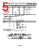
7 / 20 page  Preliminary Technical Data AD5601/AD5611/AD5621 Rev. PrC | Page 7 of 20 PIN CONFIGURATION AND FUNCTION DESCRIPTIONS TOP VIEW (Not to Scale) VDD GND SCLK DIN AD5601/ AD5611/ AD5621 VOUT SYNC 1 2 3 6 5 4 Figure 3. 6-Lead SC70 Pin Configuration Table 5. Pin Function Descriptions Pin No. Mnemonic Function 1 SYNC Level-Triggered Control Input (Active Low). This is the frame synchronization signal for the input data. When SYNC goes low, it enables the input shift register, and data is transferred in on the falling edges of the clocks that follow. The DAC is updated following the 16th clock cycle unless SYNC is taken high before this edge, in which case the rising edge of SYNC acts as an interrupt and the write sequence is ignored by the DAC. 2 SCLK Serial Clock Input. Data is clocked into the input shift register on the falling edge of the serial clock input. Data can be transferred at rates up to 30 MHz. 3 DIN Serial Data Input. This device has a 16-bit shift register. Data is clocked into the register on the falling edge of the serial clock input. 4 VDD Power Supply Input. The AD5601/AD5611/AD5621 can be operated from 2.7 V to 5.5 V. VDD should be decoupled to GND. 5 GND Ground Reference Point for All Circuitry on the AD5601/AD5611/AD5621. 6 VOUT Analog Output Voltage from the DAC. The output amplifier has rail-to-rail operation. |
|
|
Link URL |
| Cho đến nay ALLDATASHEET có giúp ích cho doanh nghiệp của bạn hay không? [ DONATE ] |
Alldatasheet là | Quảng cáo | Liên lạc với chúng tôi | Chính sách bảo mật | Liên kết đến bảng dữ liệu | Trao đổi link | Tìm kiếm theo nhà sản xuất All Rights Reserved©Alldatasheet.com |
| Russian : Alldatasheetru.com | Korean : Alldatasheet.co.kr | Spanish : Alldatasheet.es | French : Alldatasheet.fr | Italian : Alldatasheetit.com Portuguese : Alldatasheetpt.com | Polish : Alldatasheet.pl | Vietnamese : Alldatasheet.vn Indian : Alldatasheet.in | Mexican : Alldatasheet.com.mx | British : Alldatasheet.co.uk | New Zealand : Alldatasheet.co.nz |
|
Family Site : ic2ic.com |
icmetro.com |
 Vietnamese ▼
 English
 Chinese
 German
 Japanese
 Russian
 Korean
 Spanish
 French
 Italian
 Portuguese
 Polish
 Vietnamese
 Indian
 Mexican
 British
 New Zealand