 |
công cụ tìm kiếm bảng dữ liệu linh kiện điện tử |
|
|
công cụ tìm kiếm bảng dữ liệu linh kiện điện tử |
|
The question interval is too short.
Please try again in a few seconds.

Hello, Please ask a question about SN54HC74 Datasheet
# Example questions:
➢ Give two examples of these urls, categorized by whether they relate to 'products' or 'applications'.
➢ What is the purpose of figure 1 in the document, and what key elements does it illustrate?
➢ What is the primary application area where texas instruments explicitly advises against using their products without a specific agreement?
| Part No. | SN54HC74 |
| Manufacturer | TI |
| Size | 733 Kbytes |
| Pages | 20 pages |
| Description | DUAL D-TYPE POSITIVE-EDGE-TRIGGERED FLIP-FLOPS WITH CLEAR AND PRESET |

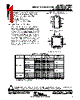




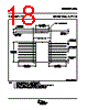


# SN54HC74 / SN74HC74 Dual D-Type Positive-Edge-Triggered Flip-Flops
## Features & Description
️· Function: Dual D-type positive-edge-triggered flip-flops with clear and preset.
️· Logic: Data is transferred on the positive-going edge of the clock pulse. Clear (CLR) and Preset (PRE) inputs override other inputs.
️· Operating Voltage: 2V to 6V
️· Applications: General-purpose logic, data storage, shift registers.
## Electrical Characteristics
️· Input Voltage (VI): 0V to VCC
️· Output Voltage (VO): 0V to VCC
️· Absolute Maximum Ratings: VCC (–0.5V to 7V), Input/Output Clamp Current (±20mA).
️· Recommended Operating Conditions: VCC (2V-6V), Operating Temperature (-55°C to 85°C / -40°C to 85°C).
## Timing Requirements
️· Clock Frequency (fclock): Up to 36 MHz (depending on VCC).
️· Setup Time (tsu): Minimum time data must be stable before clock edge.
️· Hold Time (th): Minimum time data must remain stable after clock edge.
️· Pulse Duration (tw): Minimum pulse width for PRE/CLR signals.
## Package Options
️· CDIP (J)
️· CFP (W)
️· LCCC (FK)
️· PDIP (N)
️· SOIC (D)
️· SSOP (DB)
️· TSSOP (PW)
## Ordering Information
️· Various package and temperature grade options available (e.g., SN74HC74N, SN74HC74D, SN74HC74DR).
️· Military grade versions also available (e.g., SNJ54HC74J).
# SN54HC74 / SN74HC74 Dual D-Type Positive-Edge-Triggered Flip-Flops
## Features & Description
️· Function: Dual D-type positive-edge-triggered flip-flops with clear and preset.
️· Logic: Data is transferred on the positive-going edge of the clock pulse. Clear (CLR) and Preset (PRE) inputs override other inputs.
️· Operating Voltage: 2V to 6V
️· Applications: General-purpose logic, data storage, shift registers.
## Electrical Characteristics
️· Input Voltage (VI): 0V to VCC
️· Output Voltage (VO): 0V to VCC
️· Absolute Maximum Ratings: VCC (–0.5V to 7V), Input/Output Clamp Current (±20mA).
️· Recommended Operating Conditions: VCC (2V-6V), Operating Temperature (-55°C to 85°C / -40°C to 85°C).
## Timing Requirements
️· Clock Frequency (fclock): Up to 36 MHz (depending on VCC).
️· Setup Time (tsu): Minimum time data must be stable before clock edge.
️· Hold Time (th): Minimum time data must remain stable after clock edge.
️· Pulse Duration (tw): Minimum pulse width for PRE/CLR signals.
## Package Options
️· CDIP (J)
️· CFP (W)
️· LCCC (FK)
️· PDIP (N)
️· SOIC (D)
️· SSOP (DB)
️· TSSOP (PW)
## Ordering Information
️· Various package and temperature grade options available (e.g., SN74HC74N, SN74HC74D, SN74HC74DR).
️· Military grade versions also available (e.g., SNJ54HC74J).
| Part No. | SN54HC74 |
| Manufacturer | TI |
| Size | 733 Kbytes |
| Pages | 20 pages |
| Description | DUAL D-TYPE POSITIVE-EDGE-TRIGGERED FLIP-FLOPS WITH CLEAR AND PRESET |
| Cho đến nay ALLDATASHEET có giúp ích cho doanh nghiệp của bạn hay không? [ DONATE ] |
Alldatasheet là | Quảng cáo | Liên lạc với chúng tôi | Chính sách bảo mật | Liên kết đến bảng dữ liệu | Trao đổi link | Tìm kiếm theo nhà sản xuất All Rights Reserved©Alldatasheet.com |
| Russian : Alldatasheetru.com | Korean : Alldatasheet.co.kr | Spanish : Alldatasheet.es | French : Alldatasheet.fr | Italian : Alldatasheetit.com Portuguese : Alldatasheetpt.com | Polish : Alldatasheet.pl | Vietnamese : Alldatasheet.vn Indian : Alldatasheet.in | Mexican : Alldatasheet.com.mx | British : Alldatasheet.co.uk | New Zealand : Alldatasheet.co.nz |
|
Family Site : ic2ic.com |
icmetro.com |
 Vietnamese ▼
  English
 Chinese
 German
 Japanese
 Russian
 Korean
 Spanish
 French
 Italian
 Portuguese
 Polish
 Indian
 Mexican
 British
 New Zealand