 |
công cụ tìm kiếm bảng dữ liệu linh kiện điện tử |
|
|
công cụ tìm kiếm bảng dữ liệu linh kiện điện tử |
|
The question interval is too short.
Please try again in a few seconds.

Hello, Please ask a question about APT20M16B2FLL_04 Datasheet
# Example questions:
➢ What is the typical value for the gate-source threshold voltage (vgs(th)) based on figure 9?
➢ What is the approximate maximum safe operating area (vds, id) for a device operating at a junction temperature of +25°c?
➢ How does increasing the gate resistance (rg) affect the switching energy (eon/eoff) as shown in figure 17?
| Part No. | APT20M16B2FLL_04 |
| Manufacturer | ADPOW |
| Size | 165 Kbytes |
| Pages | 5 pages |
| Description | POWER MOS 7 FREDFET |

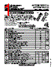

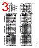
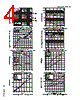


Okay, here's a breakdown of the provided image data, aiming to summarize the key information and technical details contained within the device datasheet/specification sheet.
Device: APT20M16B2FLL_LFLL (likely a MOSFET - Metal-Oxide-Semiconductor Field-Effect Transistor)
General Characteristics & Key Parameters
️· Voltage: VDD = 133V (This likely refers to the drain-source voltage in many of the figures)
️· Current: ID = 100A (drain current)
️· Temperature: TJ = 125°C (Junction Temperature), TJ = 133V (in some plots to show behavior at various temperatures)
️· Gate Resistance: RG = 5 Ohms (in switching plots)
️· L: Inductance values vary (100µH, 10µH) used in switching plots
Important Notes & Limitations Found in the Documentation
️· EON includes reverse recovery: The EON time (Turn-On time) includes the reverse recovery time of the internal diode. This is a significant factor in switching applications and must be considered in circuit design.
️· Switching Plots have multiple setups: Many plots involve specific combinations of voltage, gate resistance, inductance, and temperature. This means the data isn't a universal truth; it's conditional on these parameters.
Figure Summaries
Here's a breakdown of what each figure is likely illustrating:
️· Fig. 2: Maximum Safe Operating Area (SOA): Shows the maximum drain voltage and drain current that the device can handle without damage. Critical for reliable operation.
️· Fig. 3: Capacitance vs. Drain-to-Source Voltage: Illustrates how various capacitances (Ciss, Coss, Crss) change with Vds. These capacitances affect switching speed.
️· Fig. 5: Gate Charges vs. Gate-to-Source Voltage: Shows how total gate charge (Qg) varies with Vgs. This impacts gate drive requirements.
️· Fig. 6: Source-Drain Diode Forward Voltage: Shows the voltage drop across the internal diode when conducting current.
️· Fig. 8: Delay Times vs. Current: Shows how turn-on delay time (td(on)) and turn-off delay time (td(off)) change with drain current.
️· Fig. 11: Rise and Fall Times vs. Current: Displays how switching rise time (tr) and fall time (tf) change with current.
️· Fig. 13: Switching Energy vs. Current: Shows how switching energy changes with drain current.
️· Fig. 15: Switching Energy vs. Gate Resistance: Illustrates how switching energy changes with gate resistance.
Overall Interpretation
The document describes a robust MOSFET designed for high current, fast switching applications. The internal diode's reverse recovery time is an important consideration, and careful control of gate drive and external circuitry (like inductance) is necessary to optimize switching performance and avoid damage. The datasheets are not simply “specs”; they're a guide to getting the device to perform as intended within a circuit.
Device: APT20M16B2FLL_LFLL (likely a MOSFET - Metal-Oxide-Semiconductor Field-Effect Transistor)
General Characteristics & Key Parameters
️· Voltage: VDD = 133V (This likely refers to the drain-source voltage in many of the figures)
️· Current: ID = 100A (drain current)
️· Temperature: TJ = 125°C (Junction Temperature), TJ = 133V (in some plots to show behavior at various temperatures)
️· Gate Resistance: RG = 5 Ohms (in switching plots)
️· L: Inductance values vary (100µH, 10µH) used in switching plots
Important Notes & Limitations Found in the Documentation
️· EON includes reverse recovery: The EON time (Turn-On time) includes the reverse recovery time of the internal diode. This is a significant factor in switching applications and must be considered in circuit design.
️· Switching Plots have multiple setups: Many plots involve specific combinations of voltage, gate resistance, inductance, and temperature. This means the data isn't a universal truth; it's conditional on these parameters.
Figure Summaries
️· Fig. 2: Maximum Safe Operating Area (SOA): Shows the maximum drain voltage and drain current that the device can handle without damage. Critical for reliable operation.
️· Fig. 3: Capacitance vs. Drain-to-Source Voltage: Illustrates how various capacitances (Ciss, Coss, Crss) change with Vds. These capacitances affect switching speed.
️· Fig. 5: Gate Charges vs. Gate-to-Source Voltage: Shows how total gate charge (Qg) varies with Vgs. This impacts gate drive requirements.
️· Fig. 6: Source-Drain Diode Forward Voltage: Shows the voltage drop across the internal diode when conducting current.
️· Fig. 8: Delay Times vs. Current: Shows how turn-on delay time (td(on)) and turn-off delay time (td(off)) change with drain current.
️· Fig. 11: Rise and Fall Times vs. Current: Displays how switching rise time (tr) and fall time (tf) change with current.
️· Fig. 13: Switching Energy vs. Current: Shows how switching energy changes with drain current.
️· Fig. 15: Switching Energy vs. Gate Resistance: Illustrates how switching energy changes with gate resistance.
Overall Interpretation
| Part No. | APT20M16B2FLL_04 |
| Manufacturer | ADPOW |
| Size | 165 Kbytes |
| Pages | 5 pages |
| Description | POWER MOS 7 FREDFET |
| Cho đến nay ALLDATASHEET có giúp ích cho doanh nghiệp của bạn hay không? [ DONATE ] |
Alldatasheet là | Quảng cáo | Liên lạc với chúng tôi | Chính sách bảo mật | Liên kết đến bảng dữ liệu | Trao đổi link | Tìm kiếm theo nhà sản xuất All Rights Reserved©Alldatasheet.com |
| Russian : Alldatasheetru.com | Korean : Alldatasheet.co.kr | Spanish : Alldatasheet.es | French : Alldatasheet.fr | Italian : Alldatasheetit.com Portuguese : Alldatasheetpt.com | Polish : Alldatasheet.pl | Vietnamese : Alldatasheet.vn Indian : Alldatasheet.in | Mexican : Alldatasheet.com.mx | British : Alldatasheet.co.uk | New Zealand : Alldatasheet.co.nz |
|
Family Site : ic2ic.com |
icmetro.com |
 Vietnamese ▼
  English
 Chinese
 German
 Japanese
 Russian
 Korean
 Spanish
 French
 Italian
 Portuguese
 Polish
 Indian
 Mexican
 British
 New Zealand